New performance mode boosts Switch mobile clocks by 25 per cent
Digital Foundry on how developers can access more Switch GPU power, plus analysis of the recent teardown.

Mere days away from the Nintendo Switch's launch, elements of uncertainty still surround the final technical specifications for the new console - but a massive leak of Nintendo's developer documentation, along with a teardown of retail hardware by a Chinese parts firm may well have given the game away. Meanwhile, new information we've sourced reveals final tweaks Nintendo has made to hardware performance in the run-up to the console's release.
As things stand, the documentation leak - dated as it is - serves to confirm much of what we already know about the system, but the teardown is something else. What's immediately apparent is that build quality and design is excellent. The Switch is a compact, elegant but simple design. The 4310mAh, 16Whr battery takes up a good portion of the internal space and by the looks of it, third party replacements by the end-user shouldn't be too difficult. Switch is held together by screws, with no evidence of the troublesome glue used in recent smartphone and tablet designs that makes taking apart (and putting back together) the latest gadgets so much more difficult.
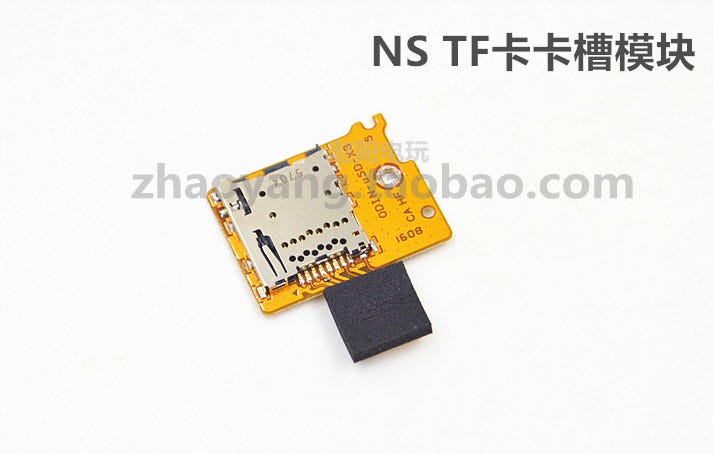
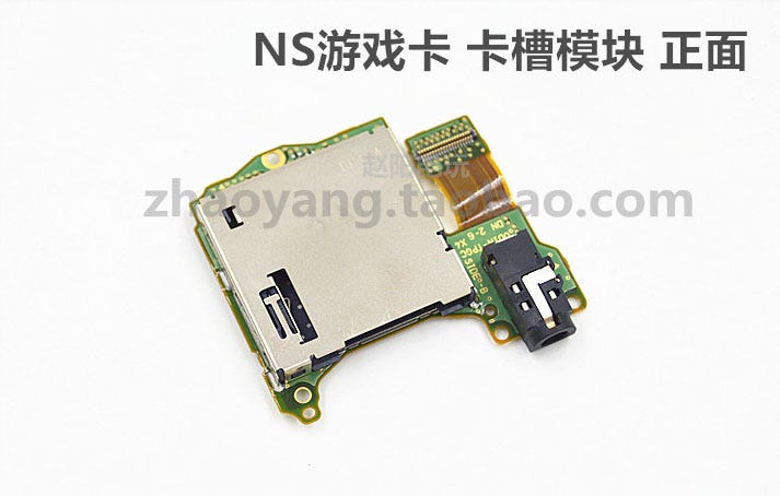
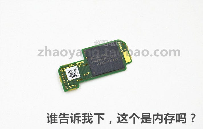
There are a few additional points we can make about the Switch's set-up based on the Chinese teardown photography - a detachable MicroSD card reader is an interesting choice, for example. It seems to sit on top of the heat-shield when the unit is first opened. Quite why Nintendo would choose to make this a replaceable part is a bit of a mystery. The 32GB of eMMC NAND storage also seems to occupy its own mini-daughterboard, as opposed to being soldered directly onto the mainboard. This offers Nintendo the chance to more easily produce premium SKUs with more generous storage capacity, while retaining the same mainboard.
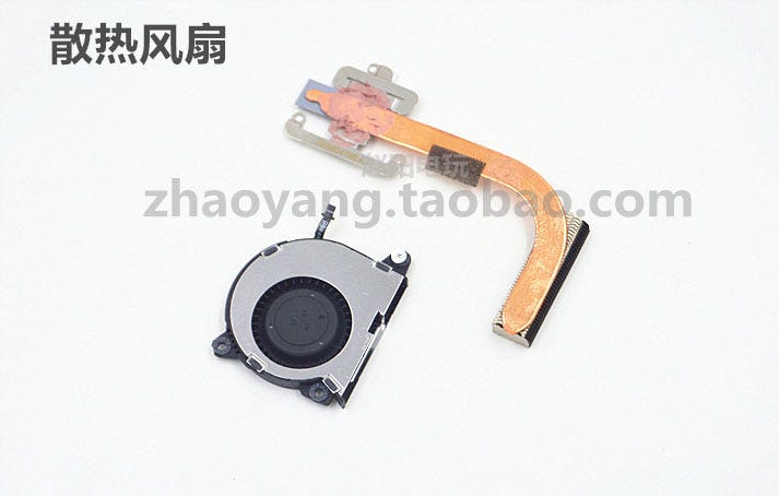
However, it's the configuration of the processor and the cooling assembly that is more intriguing. A heat pipe siphons heat away from the Nvidia Tegra processor, while active cooling is available to stop the processor overheating, ensuring consistent performance - especially in docked mode, where the GPU clocks generally rise by a factor of 2.5x. Whether the fan kicks in at all in handheld mode remains to be seen, but it's something we will be testing in our upcoming review along with its acoustic performance.

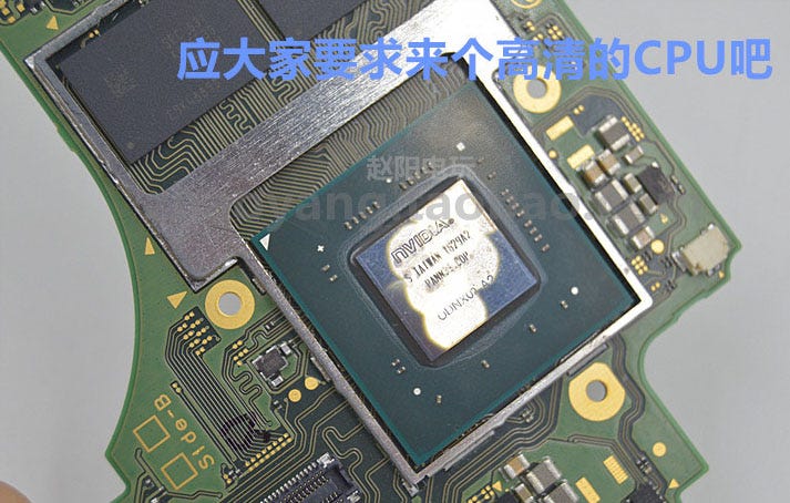
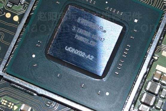
But the big question over the internals concerns the nature of the Nvidia processor itself. A couple of weeks ago, the July 2016 leak effectively handed over almost everything we need to know about the hardware, but some of the details are at odds with a very specific leak from Chinese manufacturer, Foxconn, which is clearly based on first-hand knowledge of the Switch hardware, presumably from within its production facility. With a couple of exceptions, the Foxconn leak has proved highly accurate in describing the internal configuration of the Switch right down to the shape of the heatpipe and the capacity of the battery, but it also suggests that the Nvidia Tegra processor was tested for several days straight with CPU clocks operating at 1.78GHz and the GPU pushed to 921MHz.
This is considerably higher than the clock-speeds we previously reported, representing a 20 per cent boost in terms of GPU power (921MHz vs 768MHz) and a 75 per cent bump to CPU power. In real life applications, the rise in graphics capabilities would be very useful but not exactly game-changing - but the CPU uplift certainly would change the outlook of the system's capabilities, allowing for much more complex game logic, animation and physics.
However, as much as we want the Foxconn clocks to be real, the weight of evidence is stacking up against this aspect of the leak. To maintain meaningful battery life with those clocks, we'd need to be looking at a 16nm FinFET chip and maybe even a new revision of the ARM CPU cores, and the Chinese teardown of the processor confirms that the physical size of the chip is seemingly unchanged from existing 20nm Tegra X1 SoC.
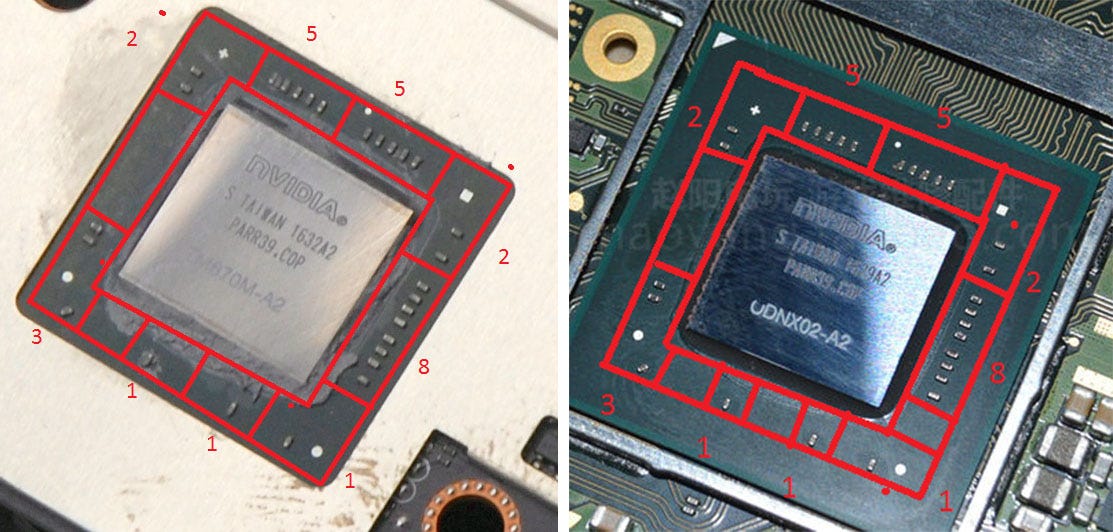
The difference between 16nm and 20nm isn't actually about transistor size, but more about the 3D 'FinFET' transistors on the lower node. A 16nm SoC would be approximately the same size as the existing 20nm Tegra X1, but the difference here is that the teardown reveals a processor with seemingly identical dimensions. Also interesting is that the processor is surrounded by the same surface-mounted arrangement of what are likely to be decoupling capacitors, there to reduce noise on the power lines. The initial conclusion we have is that we are looking at a more lightly modified X1, still on the 20nm process, which ties in more closely with the clocks we reported - and indeed every non-Foxconn spec leak seen to date.
However, there is some interesting news. While the main clock configurations for docked and undocked modes remain the same, Nintendo has added to the available performance modes available to developers in a recent update. However, we're looking at a bump to mobile GPU power, not a validation of the Foxconn clock-speeds. If the frequencies reported there were ever running on Switch, we believe they may well have been a stress test of thermal limits on the X1-derived hardware, designed to offer Nintendo a best-case scenario on just how far the processor could be pushed with its chosen cooling assembly, before finalising its retail specification. Modern consoles tend to be more conservatively clocked in order to ensure stability and reliability.
As things stand, our previously reported CPU and GPU clocks remain the default configurations for docked and handheld modes. However, having looked first-hand at a revised version of the document we previously saw in December, a new 'NX add-on' note appended to the doc introduces an expanded table of operating modes. This is how the table looks now, with the new additions in bold.

| Available CPU Speeds | Available GPU Speeds | Available Memory Controller Speeds | |
|---|---|---|---|
| Undocked | 1020MHz | 307.2MHz/384MHz | 1331.2MHz |
| Docked | 1020MHz | 307.2MHz/384MHz/768MHz | 1331.2MHz/1600MHz |
The key addition is a new mode seemingly designed to beef up handheld performance. Developers can opt for a 384MHz GPU clock - a straight 25 per cent uplift in compute power compared to the default 307.2MHz option. Both frequencies are available to developers in what it calls 'normal mode' operation - and to be clear, users will not be able to choose between them. Additionally, adjustments have been made to available memory bandwidth. In our prior story, we revealed that in undocked mode, developers could choose between running the LPDDR4 memory at either 1600MHz or 1331.2MHz. The 1600MHz option is now only available in 'boost mode' - when Switch is docked - while 1600MHz support in mobile mode is deprecated. As before, developers can opt to run handheld modes while in the dock too, and to be clear, the documentation has no new modes for docked performance. On top of that, we should stress that not all games will use the 384MHz GPU mobile mode - game-makers will choose the best fit for their projects, and 307.2MHz remains the default option.
Moving into pure speculation mode for a moment, we wonder whether Zelda uses the new mobile GPU clock mode - it closes the gap a little between handheld and docked GPU performance and combined with only a small leap in memory bandwidth, this may explain why the title renders at 720p on the go, but only 900p when docked. Beyond that, we also wonder whether using the 384MHz mode may come with compromises elsewhere in the system - perhaps by disabling WiFi (PS Vita also had multiple performance modes and one of them did turn off WiFi in order to repurpose the power budget). This is speculation of course, and as always, time will tell.
The expanded table above still shows memory frequencies in line with Tegra X1's capabilities and a look at the Chinese Switch teardown shows two Samsung LPDDR4 modules in parallel, in exactly the same configuration used in Shield Android TV. The only difference seems to come from the capacity of the RAM chips. Shield uses two 1.5GB modules, while Switch ups that to a 2x 2GB configuration for 4GB of total system memory. Identifying the exact modules used has been a lengthy topic of discussion owing to a colossal watermark obscuring the chips on the Chinese photography, but there has been some excellent detective work over at NeoGAF. The precise parts are still unconfirmed but the configuration strongly suggests a 64-bit memory bus, again tying in with the existing Switch spec leaks and ruling out the 128-bit interface used with the Pascal-based 16nm Tegra X2.

On top of all this data and analysis, we can add an additional metric on top - power consumption from the wall in docked mode, measured from final retail Switch hardware. Under load, the highest power draw we've seen so far is 16W. The launch version of the Tegra X1-powered Shield Android TV comes in at 19.5W. It should be stressed that this can only be a ballpark comparison in power consumption between the two devices - after all, clock-speeds are different and we can't compare identical content running on each device. However, if Switch were utilising a 16nm processor, the chances are that power consumption would be considerably lower.
While there is still the possibility of a more refined SoC within the retail hardware, the bottom line is that Switch has a processor that looks like a Tegra X1, with specs from Nintendo in line with X1, and power consumption that fits the characteristics of the chip's 20nm fabrication process (and power draw analysis of the second Shield revision may prove illuminating as a closer comparison point). To what extent Nintendo and Nvidia have customised the technology remains unknown - but major revisions to the hardware would almost certainly have resulted in a noticeable change in dimensions for the final silicon compared to Tegra X1, something that isn't apparent on the Switch SoC.
While the teardown photos, prior leaks and new developer documentation all point towards mature Tegra technology inside the Switch, the fact remains that this is by far and away the most powerful handheld console ever made, backed by a dedicated API designed to extract maximum performance from the hardware. However, the gulf in performance between mobile and docked configurations is considerable, which may require graphical compromises when gaming on the go.
At this point, the spec story may well have run its course, but in the run-up to launch, this is actually where things get really interesting. The Legend of Zelda: Breath of the Wild may well be the most ambitious mobile title ever made, and a great indicator of how developers will scale experiences between handheld and docked Switch configurations. Is resolution the only compromise? Next week, we'll have a full hardware review, plus detailed Zelda Switch and Wii U analysis, and we look forward to sharing our results.